Thursday, July 9, 2009

Verilog Interview Questions and Problems

Introduction :

A fresh graduate faces some tough questions in his first job interview. The questions themselves are simple but require practical and innovative approach to solve them.

What matters is your approach to solution and understanding of basic hardware design principles.


Some other pages on interview questions:

1. Electrical Engineering Technical Interview Questions/Review : This page has answers too.

2. http://enpub.fulton.asu.edu/cse517/interview.html


Recently added questions

Q. Design a memory system as shown in diagram below.

Note: Only 2000 data entries will be used at a given time. Entries should be programmable by external CPU.

Q. Create "AND" gate using a 2:1 multiplexer. (Create all other gates too.)

Q. Design XOR gate using just NAND gates.

Q. Design a "Stackable First One" finder.

Design a small unit which processes just 1 bit. Design in such a way that it can be stacked to accept make input of any length.


Q Micro architect DMA controller block for given specifications

Note:
- Overall performance should be almost same as performance of Encryption Engine which is 1Gbps.


Q. Design Gray counter to count 6.


Q. Design a block to generate output according to the following timing diagram.

Q. Design a module as shown in following block diagram.


Note: channel_id is 11 bits wide to accomodate 2K entries in 2K deep SRAM. operation is 1 bit wide.
operation = 00 means write to current location.
operation = 01 means add 1 to existing data
operation = 10 means subtract 1 from existing data in SRAM.
Do not optimize based on operation as in future operations bits can change.
Design such that you can support 1 operation every clock.

Q. Design a hardware to implement following equations without using multipliers or dividers.
out = 7x + 8y;
out = .78x + .17y;


Old Questions

Q. Create 4 bit multiplier using a ROM and what will be the size of the ROM. How can you realize it when the outputs are specified.

Q. How can you swap 2 integers a and b, without using a 3rd variable

Q. Which one is preferred? 1's complement or 2's complement and why?

Q. Which one is preferred in FSM design? Mealy or Moore? Why?

Q. Which one is preferred in design entry? RTL coding or Schematic? Why?

Q. Design a 2 input OR gate using a 2:1 mux.

Q. Design a 2 input AND gate using a 2 input XOR gate.

Q. Design a logic which mimics a infinite width register. It takes input serially 1 bit at a time. Output is asserted high when this register holds a value which is divisible by 5.

For example:

Input Sequence Value Output
1 1 1 0
0 10 2 0
1 101 5 1
0 1010 10 1
1 10101 21 0


(Hint: Use a FSM to create this)


Q. Design a block which has 3 inputs as followed.
1. system clock of pretty high freq
2. asynch clock input P
3. asynch clock input Q

P and Q clocks have 50% duty cycle each. Their frequencies are close enough and they have phase difference. Design the block to generate these outputs.

1. PeqQ : goes high if periods of P and Q are same
2. PleQ : goes high if P's period is less than that of Q.
3. PgrQ : goes high if P's period is greater than that of Q.


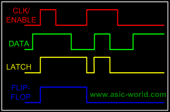
Q. What's the difference between a latch and a flip-flop? Write Verilog RTL code for each. (This is one of the most common questions but still some EE's don't know how to explain it correctly!)


Q. Design a black box whose input clock and output relationship as shown in diagram.

__ __ __ __ __ __ __ __ __
clk __| |__| |__| |__| |__| |__| |__| |__| |__| |__

__ __ __ __ __
Output __| |________| |________| |________| |________| |__


Q. Design a digital circuit to delay the negative edge of the input
signal by 2 clock cycles.
______________________
input
________| |_____________
_ _ _ _ _ _ _ _ _ _ _ _ _
clock _| |_| |_| |_| |_| |_| |_| |_| |_| |_| |_| |_| |_| |_
___________________________
output _________| |___________


Q. Design a Pattern matching block

- Output is asserted if pattern "101" is detected in last 4 inputs.
- How will you modify this design if it is required to detect same "101" pattern anywhere in last
8 samples?


Questions:

Q.

The digital circuit is shown with logic delay (dly3) and two clock buffer delays (dly1, dly2).

- How will you fix setup timing violations occurring at pin B?
- How will you fix hold violations occurring at pin B?

(Hint: Change the values of three delays to get desired effect)


Q.

Sender sends data at the rate of 80 words / 100 clocks
Receiver can consume at the rate of 8 words / 10 clocks

Calculate the depth of FIFO so that no data is dropped.
Assumptions: There is no feedback or handshake mechanism. Occurrence of data in that time period is guaranteed but exact place in those clock cycles is indeterminate.


Q

Optical sensors A and B are positioned at 90 degrees to each other as shown in Figure. Half od the disc is white and remaining is black. When black portion is under sensor it generates logic 0 and logic 1 when white portion is under sensor.

Design Direction finder block using digital components (flip flops and gates) to indicate speed. Logic 0 for clockwise and Logic 1 for counter clockwise.


Q

Will this design work satisfactorily?
Assumptions: thold = tsetup = tclock_out = tclock_skew = 1ns.
After reset A = 0, B = 1


Q. Design a 4:1 mux in Verilog.
      4:1 MUX
  • Multiple styles of coding. e.g.

  • Using if-else statements

    if(sel_1 == 0 && sel_0 == 0) output = I0;
    else if(sel_1 == 0 && sel_0 == 1) output = I1;
    else if(sel_1 == 1 && sel_0 == 0) output = I2;
    else if(sel_1 == 1 && sel_0 == 1) output = I3;

    Using case statement

    case ({sel_1, sel_0})
    00 : output = I0;
    01 : output = I1;
    10 : output = I2;
    11 : output = I3;
    default : output = I0;
    endcase

  • What are the advantages / disadvantages of each coding style shown above?
  • How Synthesis tool will give result for above codes?
  • What happens if default statement is removed in case statement?
  • What happens if combination 11 and default statement is removed? (Hint Latch inference)

  • (Comments : Though this questions looks simple and out of text books, the answers to supporting questions can come only after some experience / experimentation.)

Q. Design a FSM (Finite State Machine) to detect a sequence 10110.

  • Have a good approach to solve the design problem.
  • Know the difference between Mealy, Moore, 1-Hot type of state encoding.
  • Each state should have output transitions for all combinations of inputs.
  • All states make transition to appropriate states and not to default if sequence is broken. e.g. S3 makes transition to S2 in example shown.
  • Take help of FSM block diagram to write Verilog code.

Q. One more sequence detector:

Design a FSM (Finite State Machine) to detect more than one "1"s in last 3 samples.
For example: If the input sampled at clock edges is 0 1 0 1 0 1 1 0 0 1
then output should be 0 0 0 1 0 1 1 1 0 0 as shown in timing diagram.

And yes, you have to design this FSM using not more than 4 states!!

Sequence Detector Timing Diagram


Q. Design a state machine to divide the clock by 3/2.

frequency divider

(Hint: 2 FSMs working on posedge and negedge)


Q. Draw timing diagrams for following circuit.

Diagram of cascaded flip-flops

Timing Diagram

  • What is the maximum frequency at which this circuit can operate?
  • What is the minimum width of input pulse and position?
  • Problem can be given interesting twist by specifying all delays in min and max types.

Q. Design a Digital Peak Detector in Verilog.

Peak Detector Diagrams


Q. Design a RZ (return to zero )circuit. Design a clock to pulse circuit in Verilog / hardware gates.

Return to Zero Circuit


Q. Miscellaneous Basic Verilog Questions:

  • What is the difference between Behavior modeling and RTL modeling?
  • What is the benefit of using Behavior modeling style over RTL modeling?
  • What is the difference between blocking assignments and non-blocking assignments ?
  • How do you implement the bi-directional ports in Verilog HDL
  • How to model inertial and transport delay using Verilog?
  • How to synchronize control signals and data between two different clock domains?

Tuesday, April 28, 2009

Verilog PLI

Designers have employed HDLs for more than a decade, using them to replace a schematic-based design methodology and to convey design ideas. Verilog and VHDL are the two most widely used HDLs for electronics design. Verilog has approximately 35,000 active designers who have completed more than 50,000 designs using Cadence's (www.cadence.com) Verilog software suite.

Even with Verilog's success, many seasoned Verilog users still perceive its programming-language interface (PLI) as a "software task" (www.angelfire.com/ca/verilog, www.europa.com/~celiac/pli.html, Reference 1). A step-by-step approach helps you "break the ice" when writing PLI functions. By learning the essentials of PLI design without getting bogged down by too many details, you will acquire a basic knowledge of PLI that you can immediately use.

Why should you use a PLI?

A PLI gives you an application-program interface (API) to Verilog. Essentially, a PLI is a mechanism that invokes a C function from Verilog code. People usually call the construct that invokes a PLI routine in Verilog a "system task" or "system function" if it is part of a simulator and a "user-defined task" or "user-defined function" if the user writes it. Because the essential mechanism for a PLI remains the same in both cases, this article uses the term "system call" to indicate both constructs. Examples of common system calls that most Verilog simulators include are $display, $monitor, and $finish.

You use a PLI primarily for doing tasks that would otherwise be impossible to do using Verilog syntax. For example, IEEE Standard1364-1995 Verilog has a predefined construct for doing a file write, ($fwrite, which is another built-in system call written using a PLI), but it does not have one for reading a register value directly from a file (Reference 2). More common tasks for which PLI is the only way to achieve the desired results include writing functional models, calculating delays, and getting design information. (For example, no Verilog construct gives the instance name of the parent of the current module in the design hierarchy.)

To illustrate the basic steps for creating a PLI routine, consider the problem in Listing 1. This problem is much simpler than a real-life problem you solve using PLI, however it shows many of the basic steps you use to build a PLI routine. When you run the Verilog in the listing, it should print the value of the register as 10 at time 100 and 3 at time 300. You can think of creating a PLI routine as a two-step process: First, you write the PLI routine in C; then, you compile and link this routine to the simulator's binary code.

Writing a PLI routine

The way a PLI routine interfaces with the simulator varies from simulator to simulator, although the main functions remain the same. This article discusses the interfacing mechanisms of the two most popular commercial simulators, Cadence's Verilog-XL (Reference 3) and Synopsys' (www.synopsys.com) VCS (Reference 4). Although other commercial simulators support PLI, their interfacing mechanisms do not differ significantly from these two. Over the years, Verilog PLI has evolved into PLI 1.0 and Verilog Procedural Interfaces (VPI) (see sidebar "A short history of Verilog PLI"). This article covers only PLI 1.0. Despite the differences in interfacing parts and versions, you can break down the creation of a PLI routine into four main steps.

Step 1: Include the header files

By convention, a C program implements a PLI routine in a file veriuser.c. Although you can change this name, the vconfig tool assumes this default name while generating the compilation script in a Verilog-XL environment. For now, assume that you keep the PLI routine in the file veriuser.c.

In a Verilog-XL environment, the file veriuser.c must start with the following lines:

In a VCS environment, the file must start with:

These header files contain the most basic data structures of the Verilog PLI that the program will use.

Step 2: Declare the function prototypes and variables

A PLI routine consists of several functions. Just as you would for a normal C program, you should place the prototype declarations for the functions before the function definitions. For this case, the function appears as:

In the above function, the int prototype declaration implies that these functions return an integer at the end of their execution. If there is no error, the normal return value is 0. However, if the functions are in separate files, you should declare them as external functions with:

A typical PLI routine, like any other C program, may need a few other housekeeping variables.

Step 3: Set up the essential data structures

You must define a number of data structures in a PLI program. A Verilog simulator communicates with the C code through these variables. Open Verilog International (OVI) (www.ovi.org/pubs.html), an organization for standardizing Verilog, recommends only one mandatory data structure, veriusertfs. However, the exact number and syntax of these data structures vary from simulator to simulator. For example, Verilog-XL requires four such data structures and their functions for any PLI routine to work; VCS needs none of them and instead uses a separate input file.

The main interfacing data structure for Verilog-XL is an array of structures or a table called veriusertfs. Verilog-XL uses this table to determine the properties associated with the system calls that correspond to this PLI routine. The simulator does not recognize any names other than veriusertfs. Each element of veriusertfs has a distinct function, and you need all these functions to achieve the overall objective of correctly writing the PLI routine. The number of rows in veriusertfs is the same as the number of user-defined system calls plus one for the last entry, which is a mandatory 0. In this case, the veriusertfs array should look like:

The first entry, usertask, indicates that the system call does not return anything. It is equivalent to procedure in Pascal or function returning void in C.

In the previous data-structure, my_ checktf and my_calltf are the names of the two functions that you use to implement the system call $print_reg. These names are arbitrary, and you can replace them with other names. The function my_checktf is generally known as a checktf routine. It checks the validity of the passed parameters. Similarly, my_calltf, which you usually call calltf routine, performs the main task of the system call. The positions of these names in veriusertfs are very important. For example, if you want to use my_checkt for any other name as a checking function, it must be the third element. The function veriusertfs provides options for a few other user-defined functions that you will not use in this routine. A zero replaces any function that you do not use. Therefore, the second, fourth, and sixth elements in the entry are zeroes. Table 1 summarizes the objectives of each entry in a row of veriusertfs. If there are additional system calls, you need to define a separate entry in veriusertfs for each one.

Verilog-XL also needs the following variables or functions:

The first variable, veriuser_version_str, is a string indicating the application's user-defined-version information. A bool (Boolean) variable is an integer subtype with permitted values 0 and 1. In most cases, you can use Cadence-supplied default values for these variables or functions.

In VCS, instead of a table, you use the equivalent information in a separate file, which you usually call pli.tab. This name is also user-defined. In the current example using $print_reg, the contents of this file are:

Step 4: The constituent functions

With the prototype declarations in place, you are ready to write the two functions, my_checktf() and my_calltf(), which constitute the main body of the PLI application.

As previously discussed, a checktf routine checks the validity of passed parameters. It is a good practice to check whether the total number of parameters is the same as you expect, and whether each parameter is required. For example, in this case, you expect the program to pass only one parameter of type register. You do this task in the function my_checktf() (Listing 2).

The functions starting with tf_ are the library functions and are commonly known as utility routines. The library functions in the previous function and their usage are tf_nump(), which determines how many parameters you are passing, and tf_typep(), which determines the parameter type by its position in the system call in the Verilog code. In this case, the system call is $print_reg.

Thus, tf_typep(1) gives the type of the first parameter, tf_typep(2) gives the type of the second parameter, and so on. If the parameter does not exist, tf_typep() returns an error. (In this case, tf_typep(2) does not exist.) In the current example, you expect the program to pass a register value as a parameter. Therefore, the type should be tf_readwrite. If a wire is the expected parameter, the type should be tf_readonly. To facilitate error-condition checking, it is a good idea to first check the number of parameters and then to check their types. The tf_error() function prints an error message and signals the simulator to increment its error count. These library functions and constants are parts of the header files that you have included at the top of the file in Step 1.

A calltf function is the heart of the PLI routine. It usually contains the main body of the PLI routine. In this case, it should read the value of the register and then print this value. The following code shows how you can accomplish this job:

In the above code, io_printf() does the same job as printf() in C, printing the value in standard output. Additionally, the function prints the same information in the Verilog log file. The function tf_getp() gets the register's integer value. The function tf_gettime() returns the current simulation time and needs no input parameter. Calltf is the most complicated function in a PLI routine. It often runs for several hundred lines.

Now that you have created the two main functions, you need to put them into one place. Listing 3 shows how to implement $print_reg in a Verilog-XL environment.

The next task is making the Verilog simulator understand the existence of your new system call. To accomplish this task, you must compile the PLI routine and then link it to the simulator's binary. Although you can manually integrate the PLI code with the Verilog binary by running a C compiler and merging the object files, it is more convenient to use a script. In Verilog-XL, a program called vconfig generates this script. The default name for this script is cr_vlog. While generating this script, the program vconfig asks for the name of the compiled Verilog that you prefer. It also asks whether to include model libraries, which are PLI code, from standard vendors. For most of these questions, the default answer, which you input if you press return without entering anything, is good enough unless you have a customized environment. At the end, vconfig asks for the path for your veriuser.c files. Once you generate the script cr_vlog, you need only to run the script to generate a customized Verilog simulator that can execute the new system call.

A sample run of the compiled Verilog using this PLI routine produces the output with a Verilog-XL simulator (Listing 4).

Modifying the value of a register

You use a PLI is to read design information and to modify this information in the design database. The following example shows how you can do this modification. Create a system call, $invert, to print the value of a register (as in the previous example), bitwise invert the content, and print this updated value. Many ways exist to invert a value of a binary number. By using a straightforward algorithm to do the inversion, as the following list shows, helps you gain more insight into the PLI mechanism and library functions:

  • read the content of the register as a string;
  • convert all ones in the string to twos, convert all zeros to ones, convert all twos to zeros, convert all Z's to X's, and leave X's intact; and
  • put the modified string back into the register.

The second step converts all ones to zeros and zeros to ones. Note that the checktf function in this case does not differ from the earlier one, because in both cases the number and type of input parameter are the same.

Creating the PLI routine

Listing 5 shows the implementation of $invert routine in a VCS environment. This program uses the following library functions:

  • tf_strgetp() returns the content of the register as a string. Just liketf_getp(), it reads the register's content as a decimal. In Listing 5, tf_strgetp(1, b) reads the content of the first parameter in binary format. (An h or o, in place of a b, read it in hexadecimal or octal format, respectively). The routine then copies the content to a string val_string.
  • tf_strdelputp() writes a value to a parameter from a string-value specification. This function takes a number of arguments, including the parameter index number (the relative position of the parameters in the system call, starting with 1 for the parameter on the far left); the size of the string whose value the parameter contains (in this case, it should be same size as the register); the encoding radix; the actual string; and two other delay-related arguments, which you ignore by passing zeros for them. Although not shown in the current example, a simpler decimal counterpart of tf_strdelputp() is tf_putp().

It is important to remember that a program can change or overwrite only the value of certain objects from a PLI routine. Any attempt to change a variable that you cannot put on the left of a procedural assignment in Verilog, such as a wire, results in an error. In general, you can modify the contents of a variable of type tf_readwrite. The checktf function my_checktf() checks this feature.

One additional user-defined function that Listing 5 uses is move(), which has three parameters. In the third parameter, a string, the second parameter replaces every occurrence of the first parameter. In the current case, a series of calls to move() changes the zeros to ones and ones to zeros. However, once a program converts zeros to ones, you must distinguish the converted ones in the string from the original ones. To make this distinction, the program first changes all initial ones to twos. A two is an invalid value for binary logic, but you can use it in an intermediate step for this example. At the end, the program converts all twos back to zeros. The program completes its task by putting the inverted value back into the register using the tf_strdelputp() function.

Listing 6 shows a sample Verilog program containing the call $invert. In a VCS environment, a file lists the functions associated with a PLI routine. Although this file can have any name, you usually call it pli.tab. This file is equivalent to the veriusertfs[] structure in Verilog-XL. The content of this file in the current example is:

By saving this program in the file test.v, you generate an executable binary pli_invert with the command:

Executing pli_invert, you get:

You now know the basic structure of a PLI routine and the mechanism of linking it to build a custom version of Verilog. You can also read, convert, and modify the values of the elementary components of a design database in Verilog through a PLI routine and read the simulation time for the routine. These tasks are the basic and often most necessary ones for a PLI routine to carry out. Considering all that PLI offers, this information is just the tip of the iceberg. You can also use a PLI to access design information other than register contents.


REFERENCE

1. Principles of Verilog PLI, Kluwer Academic Publisher, 1999, ISBN 0-7923-8477-6, www.wkap.nl.

2.IEEE Standard 1364-1995, IEEE Standard Hardware Description Language based on the Verilog Hardware Description Language, IEEE Press, ISBN 1-55937-727-5, www.ieee.org.

3. Verilog-XL Reference Manual, Cadence Design Systems.

4. VCS/VCSi Users Guide, Synopsys.

5.Verilog FAQ.

6. Balph, Tom, and Pat O'Malley, "C modeling accelerates HDL-system growth," EDN, Oct 22, 1998, pg 139.

Tuesday, February 24, 2009

DIGITAL DESIGN INTERVIEW QUESTIONS

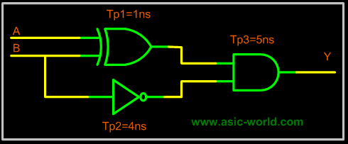
1. What is the output of AND gate in the circuit below, when A and B are as in waveform? Tp is the gate delay of respective gate.
Ans. 
../images/digital/questi4.gif


2. Identify the circuit below, and its limitation.
Ans. 
../images/digital/question_parity.gif

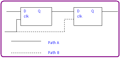
3. Referring to the diagram below, briefly explain what will happen if the propagation delay of the clock signal in path B is much too high compared to path A. How do we solve this problem if the propagation delay in path B can not be reduced ?
Ans
../images/digital/question_ff_delay.gif

4.  What is the function of a D flip-flop, whose inverted output is connected to its input ?
5.   Design a circuit to divide input frequency by 2.
6.  
What are the different types of adder implementations ?
7. What are the different types of adder implementations ?
8. Give the truth table for a Half Adder. Give a gate level implementation of it.
9. What is the purpose of the buffer in the circuit below, is it necessary/redundant to have a buffer ?
10.  What is the output of the circuit below, assuming that value of 'X' is not known ?

../images/digital/question_xor.gif
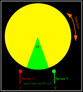
11. Consider a circular disk as shown in the figure below with two sensors mounted X, Y and a blue shade painted on the disk for an angle of 45 degree. Design a circuit with minimum number of gates to detect the direction of rotation
../images/digital/dquest_circular.gif

12. 
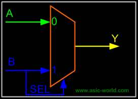
Design an OR gate from 2:1 MUX.(This is one of the most commonly asked interview questions)
Ans. 
../images/digital/mux_or.gif

13. 
Design an XOR gate from 2:1 MUX and a NOT gate
14. What is the difference between a LATCH and a FLIP-FLOP ?
Ans. 
  • Latch is a level sensitive device while flip-flop is an edge sensitive device.
  • Latch is sensitive to glitches on enable pin, whereas flip-flop is immune to glitches.
  • Latches take less gates (also less power) to implement than flip-flops.
  • Latches are faster than flip-flops. 
  • space.gif
    ../images/digital/latch_ff_wv.gif

    16.    What is metastable state ? How does it occur ?  
        
     
    17.     What is metastability ?  
        
     
    18.     Design a 3:8 decoder  
        
     
    19     Design a FSM to detect sequence "101" in input sequence.  
        
     
     20    Convert NAND gate into Inverter, in two different ways.  
        
     
      21   Design a D and T flip flop using 2:1 mux; use of other components not allowed, just the mux.  
        
     
      22   Design a divide by two counter using D-Latch.  
        
     
     23    Design D Latch from SR flip-flop.  
        
     
    24     Define Clock Skew , Negative Clock Skew, Positive Clock Skew.  
        
     
     25    What is Race Condition ?  
        
     
    26     Design a 4 bit Gray Counter.  
        
     
    27     Design 4-bit Synchronous counter, Asynchronous counter.  
        
     
     28    Design a 16 byte Asynchronous FIFO.  
        
     
     29    What is the difference between an EEPROM and a FLASH ?  
        
     
      30   What is the difference between a NAND-based Flash and a NOR-based Flash ?  
        
     
     31    You are given a 100 MHz clock. Design a 33.3 MHz clock with and without 50% duty cycle.  
        
     
     32    Design a Read on Reset System ?  
        
     
      33   Which one is superior: Asynchronous Reset or Synchronous Reset ? Explain.  
        
     
      34   Design a State machine for Traffic Control at a Four point Junction.  
        
     
      35   What are FIFO's? Can you draw the block diagram of FIFO? Could you modify it to make it asynchronous FIFO ?  
        
     
    36     How can you generate random sequences in digital circuits?  


    All these are common digital interview questions which you might come across in interviews at campus level. 


    space.gif

    Constraint to have N elements distributed in M bins

    Code to distribute N elements into M bins, you add unique keyword to have each bin will have unique number of elements. class test; param...